
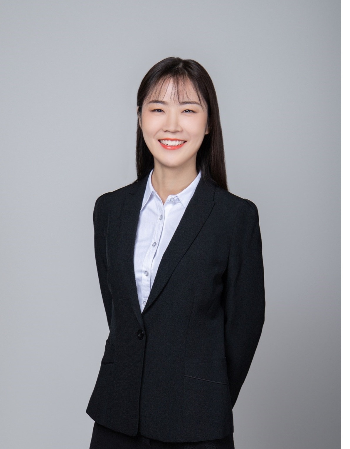
FigureAsia 35 Under 35 · Science
Can Liu
Age 33 · Wafer-scale two-dimensional electronics · China
Co-corresponding author of a 2025 Science paper on wafer-scale indium selenide and integrated transistor arrays.
- Approximate age at the edition eligibility date
- 33
- Field
- Semiconductor science
- Country or region
- China
- FigureAsia U35 Assessment
- 88.6 / 100
Profile
Career and documented record
Two-dimensional semiconductors offer excellent electrostatic control, but useful electronics require uniform material over entire wafers. In 2025, Can Liu and collaborators reported a solid–liquid–solid growth route for wafer-scale indium selenide in Science, then integrated the material into transistor arrays.
The programme combines growth chemistry, structural characterisation and device fabrication. Institutional reporting states that key measured device metrics surpassed reference three-nanometre silicon performance, a comparison that remains specific to the reported tests rather than a claim of complete process superiority.
Liu's co-corresponding authorship establishes scientific leadership within a broad team. The result matters because it confronts scale and integration together—the point at which many promising two-dimensional materials cease to look like semiconductor platforms.
FigureAsia selection
Why Can Liu is on the list
Liu is selected for moving indium selenide from attractive flakes toward wafer-scale, integrated electronics. The work is strongest where it is most concrete: growth uniformity, device arrays and measured transistor behaviour.
Verified work
The 2025–26 record
Wafer-scale InSe
Co-led a Science paper on solid–liquid–solid growth of wafer-scale two-dimensional indium selenide.
Transistor integration
Fabricated integrated arrays rather than reporting isolated exfoliated devices.
Competitive device metrics
Reported key test metrics above selected three-nanometre silicon references under stated conditions.
Field context
The work in its field
The bottleneck for two-dimensional electronics is not discovering another high-mobility flake; it is producing uniform, controllable material compatible with arrays and manufacturing workflows.
FigureAsia U35 Assessment
Assessment breakdown
88.6out of 100
Substantive 2025–2026 contribution
16.7 / 20
Co-led a Science paper on solid–liquid–solid growth of wafer-scale two-dimensional indium selenide.
Verified scientific impact
13 / 15
The Science publication brings wafer growth and integrated devices together in a field where scalability is the dominant obstacle.
Originality and distinction
9.1 / 10
The distinction lies in a solid–liquid–solid route that produces wafer-scale indium selenide suitable for transistor arrays.
Field influence
8.9 / 10
Researchers in wafer-scale two-dimensional electronics now have a stronger result to test, extend or challenge because of this contribution.
Individual agency
9.1 / 10
Liu is a co-corresponding author and institutional research leader, with growth and device work shared across the collaboration.
Durability and trajectory
4.6 / 5
The contribution builds on an active line of work at Renmin University of China, with further tests and applications still to come.
Asian significance and global relevance
4.6 / 5
Chinese physicist leading semiconductor research at Renmin University of China.
Evidential validity and reproducibility
7.1 / 8
Material characterisation and device measurements are peer reviewed; comparisons are confined to the stated metrics.
Advance in scientific knowledge
6.4 / 7
The study shows that indium selenide can be grown and controlled beyond the small-flake regime.
Translational or methodological utility
4.5 / 5
Wafer uniformity and array integration are necessary steps toward any future low-power two-dimensional electronics platform.
Responsible research stewardship
4.6 / 5
The profile refuses to rewrite selected benchmark wins as full-node commercial superiority.